Semiconductor 101: EUV - The Most Powerful Machine in Chips
How EUV lithography prints chip features, why its machines are difficult to build, and what could challenge ASML’s position.
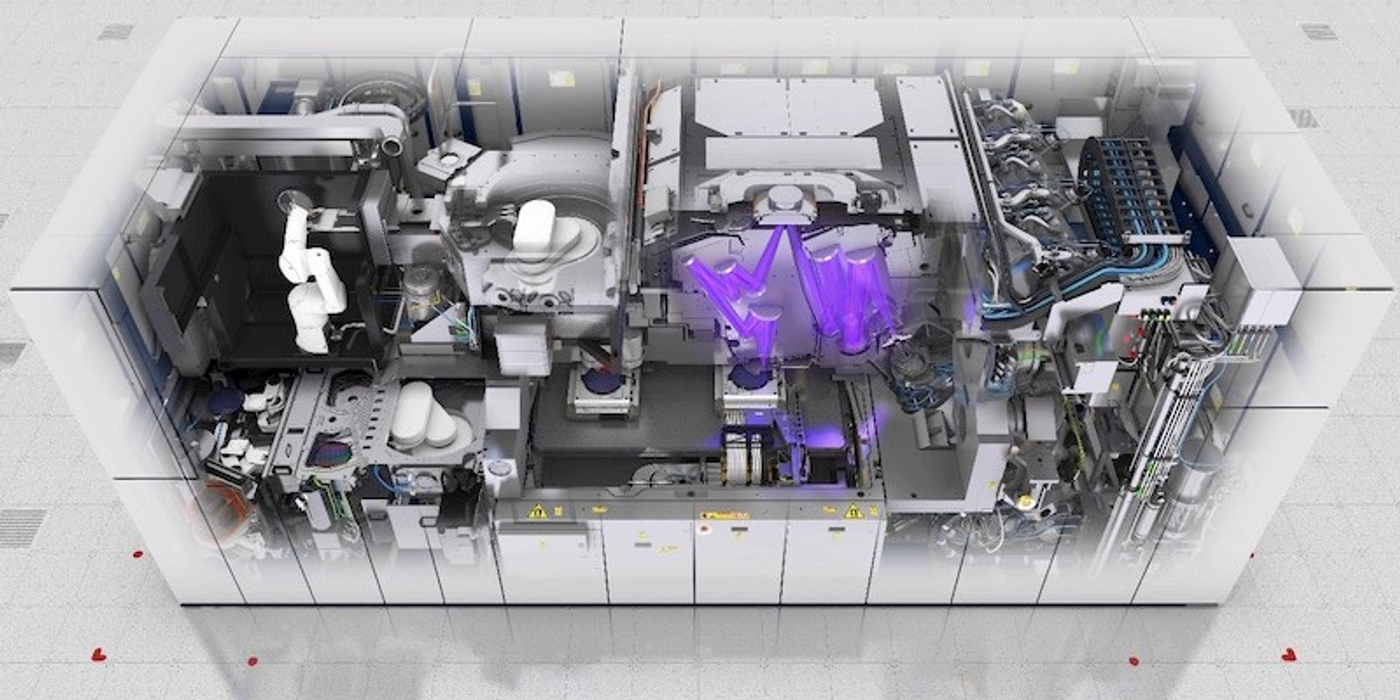
To print some of the smallest features in today’s chips, EUV machines fire lasers at molten tin and guide the resulting light through extraordinarily precise mirrors, all at factory speed and a cost of hundreds of millions of euros.
ASML alone supplies these machines for high-volume production. Understanding why means looking beyond the scanner to its physics, suppliers and economics.
1. Break down the technology
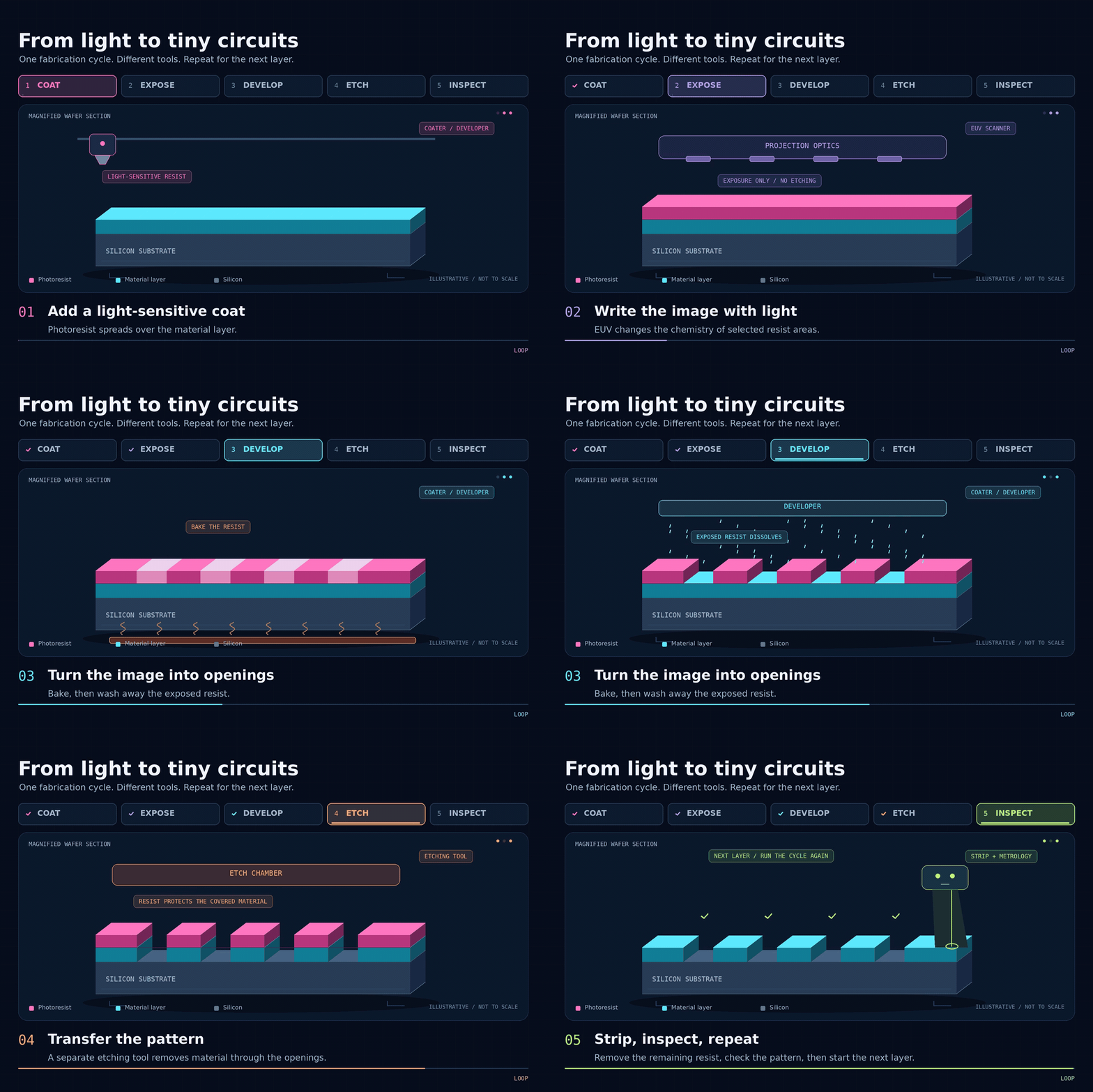
A chip is built by repeatedly adding, patterning and processing materials on a silicon wafer. Lithography defines where the patterns go. It is used during fabrication, after the chip’s circuit design has been prepared. The same wafer returns to patterning many times as transistors and connecting layers are built.
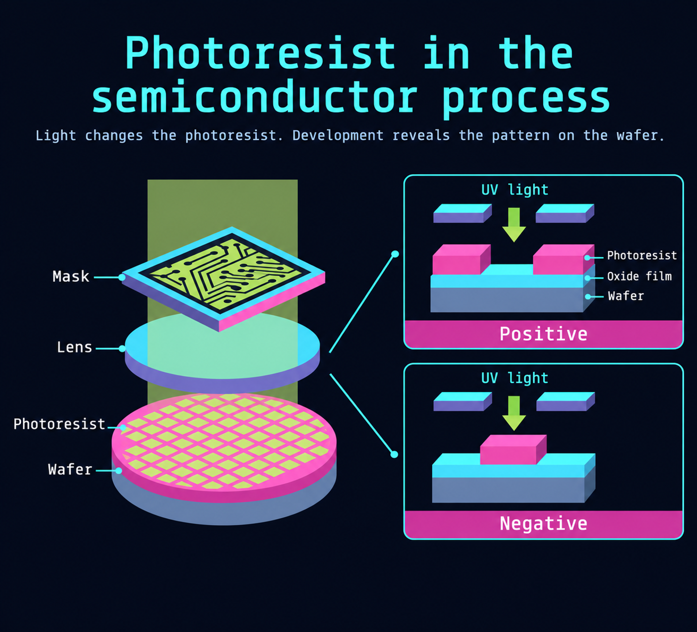
The wafer is coated with photoresist, a light-sensitive material. Light changes its chemistry; baking and development turn those changes into a physical pattern. Separate processes, such as etching, then transfer that pattern into an underlying material. The EUV scanner performs the exposure: it does not directly carve a finished circuit into silicon. Coating, development, etching and inspection require other equipment.
Why use extreme ultraviolet?
The shorter the wavelength of light, the finer the details an optical system can resolve, all else being equal. Advanced DUV systems use 193 nm light. EUV uses 13.5 nm. The optics, resist, mask and processing conditions also determine what can be printed reliably.
The distinction matters when reading chip labels. A “2 nm” manufacturing node does not mean every transistor feature is 2 nm wide. ASML quotes roughly 13 nm resolution for its conventional EUV platform and 8 nm for High NA. Those optical specifications and the name of a chip generation measure different things.
Step 1: Create the light
A droplet generator releases tiny drops of molten tin. A first laser pulse spreads a droplet out; a stronger pulse turns it into a hot plasma. That plasma emits EUV light. The drive laser itself does not emit the 13.5 nm light used to expose the wafer.
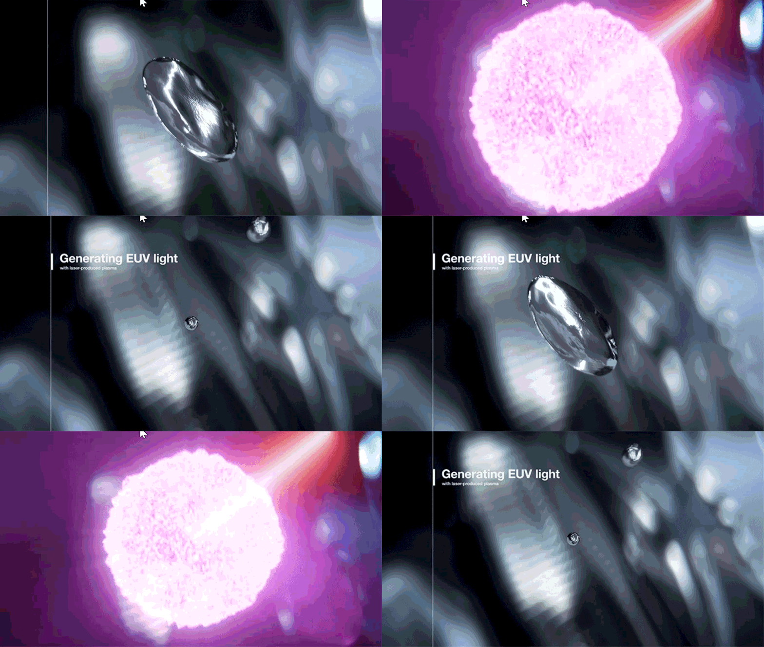
The timing is demanding: each pulse must hit a moving target with the right shape and energy. ASML’s 2025 report describes commercial sources operating at 60,000 droplets per second. Its separately reported 1,000-watt source was a demonstration, not proof that every shipped system has that capability.
Step 2: Guide and maintain the light
EUV is strongly absorbed by air and most materials, so the optical path operates in vacuum and uses mirrors rather than ordinary glass lenses. Special multilayer coatings reflect the EUV light, while exceptionally smooth surfaces limit image distortion.
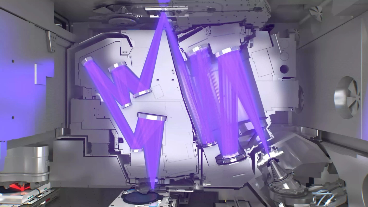
The illumination system directs light onto a reflective photomask, or reticle, carrying the pattern. Projection mirrors then form a reduced image on the resist-coated wafer. The collector, illumination optics, mask and projection optics each have their own job; this is considerably more involved than shining a lamp through a stencil.
Step 3: Keep everything aligned
The wafer and mask move during scanning. Their motion must stay synchronised while sensors and control systems correct positioning and image errors. Every new pattern must also line up with existing layers, a requirement called overlay.
Software also adjusts mask patterns to compensate for optical and chemical effects. The pattern on a mask can therefore look different from the pattern intended on the wafer. This is called computational lithography.
More source power can increase productivity, but it also raises thermal and contamination challenges. Tin debris must be managed, mirrors protected, and the resist given enough exposure to print consistently. A machine that produces a beautiful test pattern occasionally is a different proposition from one that earns its place in a working fab.
EUV is generally reserved for the most demanding layers. DUV continues to handle many others, so a modern fab needs both.
2. EUV is an industrial ecosystem
There are three different clocks: manufacturing the components, assembling and testing the scanner, and delivering and installing it for a customer. They overlap, so adding individual lead times together would be misleading.
ZEISS says the mirrors for High NA EUV take around a year to manufacture. Separately, Bloomberg reported in July 2026 that ASML’s CFO described a factory build-and-test cycle of roughly 22 weeks, with a target of 15–16 weeks. The same report put order-to-delivery time at more than a year. The shorter figure was a target, and none of these numbers is a universal build time for every model.
Delivery is a substantial operation itself. Intel’s first EXE:5000 arrived in more than 250 crates inside 43 freight containers, travelled on multiple cargo planes and required 20 trucks for the final journey to Oregon. That describes a particular installation, not a standard shipping specification for all EUV tools.
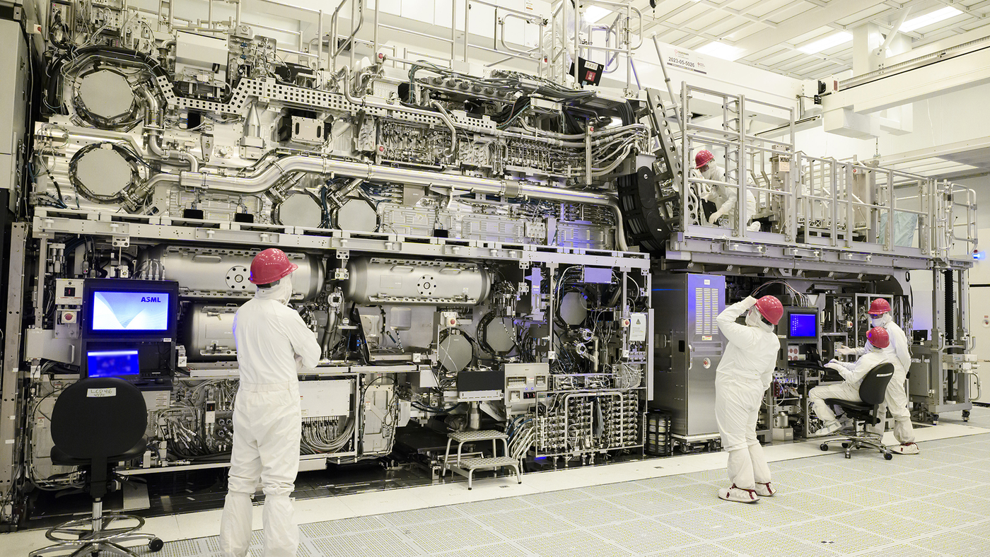
ASML has described EUV systems as containing more than 100,000 individual parts from ~40 countries. That is a useful indication of complexity, rather than a current bill of materials for every scanner generation. Its 2025 annual report lists approximately 900 product-related suppliers and 4,200 non-product-related suppliers across the company. The full 5,100 should not be described as suppliers to one EUV machine.
The EUV landscape
Selected publicly documented contributors to the scanner and its dedicated source, power and control modules. ASML operations are identified explicitly. Never a complete list though.
▣ EUV light generation
▣ Illumination and projection optics
▣ Vacuum vessel and components
▣ Precision mechanics and handling
▣ Electrical power and control
▣ Final system integration
The main connections are easy to see. ASML integrates the scanner in the Netherlands. Its San Diego operation develops the EUV source. Germany contributes TRUMPF’s drive laser, ZEISS optics and other precision capabilities. Vacuum technology includes UK-based Edwards and Switzerland’s VAT. Austria contributes IMS’s mask-writing equipment, while Japan supplies important masks, materials and process tools. Belgium’s imec helps develop and qualify the manufacturing processes around the equipment.
Some of these are independent suppliers; others are ASML operations. Masks and resists are used in the fab rather than simply being permanent parts inside the scanner. That distinction is essential to understanding what the map shows.
3. Why ASML dominates, is anyone trying another route
ASML’s strongest position is in complete, production-qualified EUV scanners. It also competes in DUV, where Nikon and Canon remain established suppliers. Treating all lithography as an ASML monopoly would miss that distinction.
Its advantage has accumulated over decades. The company and its partners had to make the source powerful and stable, manufacture the optics, control moving stages, manage defects and help customers integrate the equipment into a profitable process. Customer funding mattered too: in 2012, Intel, TSMC and Samsung agreed to contribute €1.38 billion to a five-year programme covering EUV and 450 mm lithography development. That was not an EUV-only budget.
A new entrant therefore needs more than a good light source or an impressive resolution result. It needs the surrounding system, repeatable production, customer qualification, maintenance and a credible cost per usable wafer, all of which is nearly impossible to create over the next decade.
| Organisation or effort | What it is pursuing | What that establishes | |
|---|---|---|---|
| Nikon | DUV equipment and EUV-related technologies | Nikon’s own history says it exited complete EUV-system development in 2011. It remains active in other lithography markets. | |
| Canon | Nanoimprint lithography, physically pressing a template into resist | Commercial equipment exists. In its Q1 2026 update, Canon described production-like evaluation and a target of mass-production adoption in 2027. | |
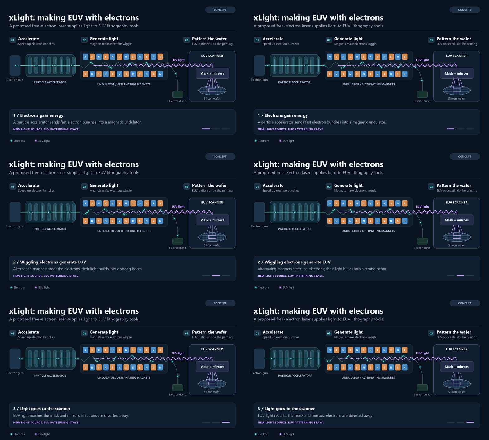
| xLight | A free-electron laser as an alternative EUV light source | A prototype programme supported by a final $150 million US CHIPS award in June 2026. It is not a complete replacement scanner. | |
| Substrate | Accelerator-generated X-ray lithography within a vertically integrated foundry | Company-published tools and patterning results; these alone do not establish sustained commercial chip yield or economics. | |
| OIST | A redesigned High NA EUV optical architecture | Published simulation work and prototype development, rather than a production-qualified scanner. | |
| Reported Chinese programme | A domestic EUV prototype | Reuters reported in December 2025 that it generated EUV light but had not produced working chips at that time. This was reporting based on unnamed sources, not a public production qualification. |
These efforts address different parts of the problem and are not equivalent competitors.
4. Could something replace EUV?
There are credible alternatives and improvements, but they solve different problems.
Canon’s nanoimprint system presses tiny circuit patterns into a coating on a silicon wafer like a stamp, rather than projecting the pattern through EUV optics. It can avoid the plasma source and EUV projection system, although UV light may still be used to harden the coating. Its main challenges are aligning successive layers, preventing defects and maintaining production speed. Canon quotes a 14 nm minimum linewidth, but that alone does not demonstrate a complete process for making leading-edge chips.
Electron beams can write extremely fine patterns directly onto a wafer without a photomask, but complex designs take a lot of time to cover. Multiple beams improve speed, and the technology already serves mask-making and specialised manufacturing, but it has not demonstrated a general replacement for EUV in high-volume chip production.
Self-assembly lets materials help form patterns. Guided by an existing pattern, materials called block copolymers organise into repeating nanoscale structures. Imec sees this as a way to extend conventional patterning, especially for regular features, but it still requires guidance and defect control, making it a complement rather than a complete replacement.
New light sources could reshape EUV lithography. xLight aims to replace the tin-plasma light source with a free-electron laser, while Substrate proposes a broader accelerator-based system; neither approach necessarily eliminates EUV projection optics.
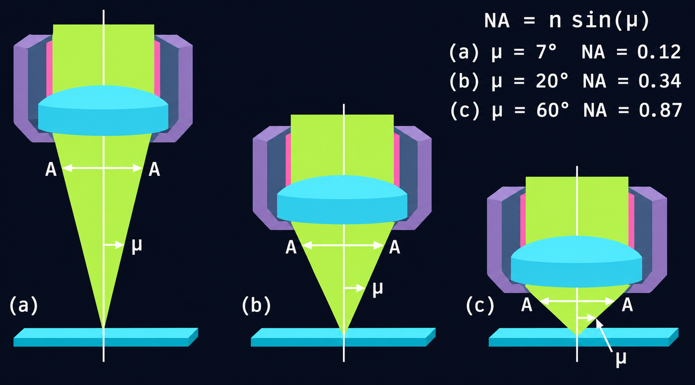
High-NA can improve EUV rather than replacing it. Raising numerical aperture from 0.33 to 0.55 lets the optics resolve finer details at the same wavelength. OIST also proposes redesigned EUV optics, but its simulations assume ideal, defect-free mirrors with perfect reflectivity, leaving substantial work before a production machine could be built.
Chiplets and 3D packaging offer another way to improve computing systems by combining or stacking dies. They can change the economics of scaling, but the individual dies still need patterned transistors and wiring.
I believe the next few years would bring a mixture of better EUV systems, more capable materials, selective use of alternative patterning and more advanced packaging. A contender will become commercially convincing when it can repeatedly make usable chips at an attractive cost and volume.